

Look at That S'Card Go!
When I got the #ForestApples many years ago, one of them came with a 16k Language Card clone in slot zero, and another RAM card in slot one. The Language Card clone had a ribbon cable going to the RAM socket at E3 as usual. The other RAM card also had its own ribbon cable going to another RAM socket! It looked like there were two Language Cards installed, something I had never seen before.
I soon discovered that the extra RAM card was a Legend Industries 64KC. It had 64k of RAM instead of a mere 16k, it could be installed into any slot to act as additional RAM, and when installed in slot zero the first 16k would appear as a normal Language Card. According to the manual though, Legend Industries had made RAM cards even larger, and being curious to see them work, I stuck a saved search into eBay so that I might find one.
Many years passed and not one single Legend RAM card ever appeared. Then a few months ago a Legend S’Card with one megabyte of RAM suddenly showed up. The seller said that all the RAM chips had been tested and they were fine, but still the card didn’t work. I was interested, but the buy-it-now price seemed a bit high for a known bad card, and I didn’t want to get into a bidding war. I watched the auction end and get relisted several times, hoping the price would go down but never did, and finally I decided that I had been waiting for a Legend card for so long I put in a bid and won it for the starting price.
 Legend Diagnostic
When the card arrived I downloaded the disks, installed the card in one of my Apple II Plus computers, booted the diagnostic, and let it run. As expected, it immediately reported problems with the card. I took the card over to my workbench and started testing all the 74xx logic ICs one-by-one using both a BackBit Chip Tester and TL866CS, and every single chip tested good. The only chip I couldn’t test was the PAL16R8, and I was worried that might be the reason the card didn’t work. The PAL16R8 is a programmable chip and if it was bad, there was no easy way to deal with it. While I could get a blank PAL16R8 and program it, I’d need to have a copy of the program, something I would be unable to get from a bad chip. And of course this card is quite rare so it wasn’t likely I’d find another.
I was starting to feel a bit overwhelmed at this point. The scanned in manual for the card didn’t include any schematics, and the diagnostic program didn’t really explain the errors it was printing. It was expected that if you had a problem with the card you would send it back to the manufacturer for them to diagnose and repair it. Since I had no schematics, no documentation on what the errors meant that the RAM test program was printing, and all the chips seemed to be good, I wasn't quite sure what to do next.
Wondering just how much of the card worked, I decided to try out some of the other demo programs that were on the disk. One of them was a slide show program which would load a bunch of 8k images from disk, copy them off to the card, and then demonstrate how much faster RAM is than a floppy drive by displaying the images in succession as quickly as possible.
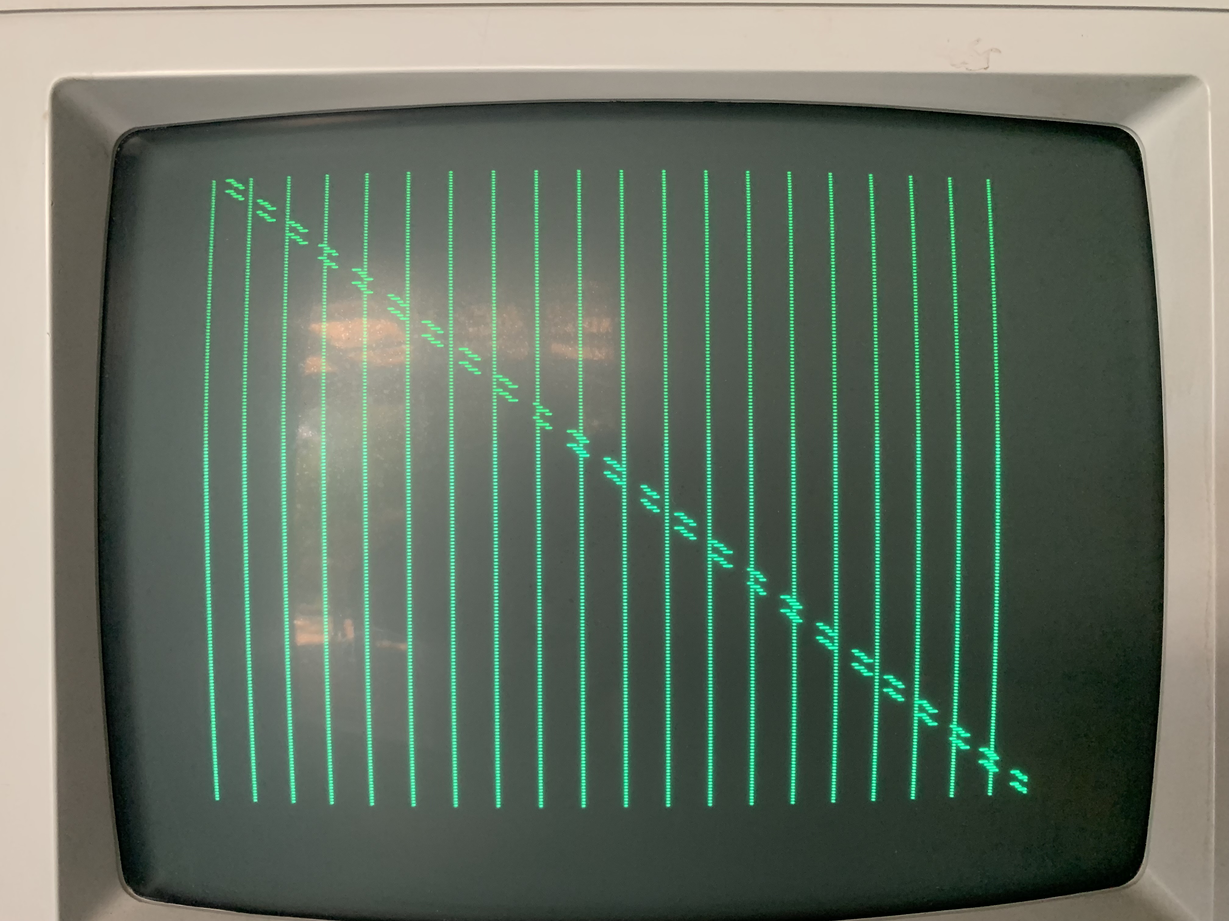
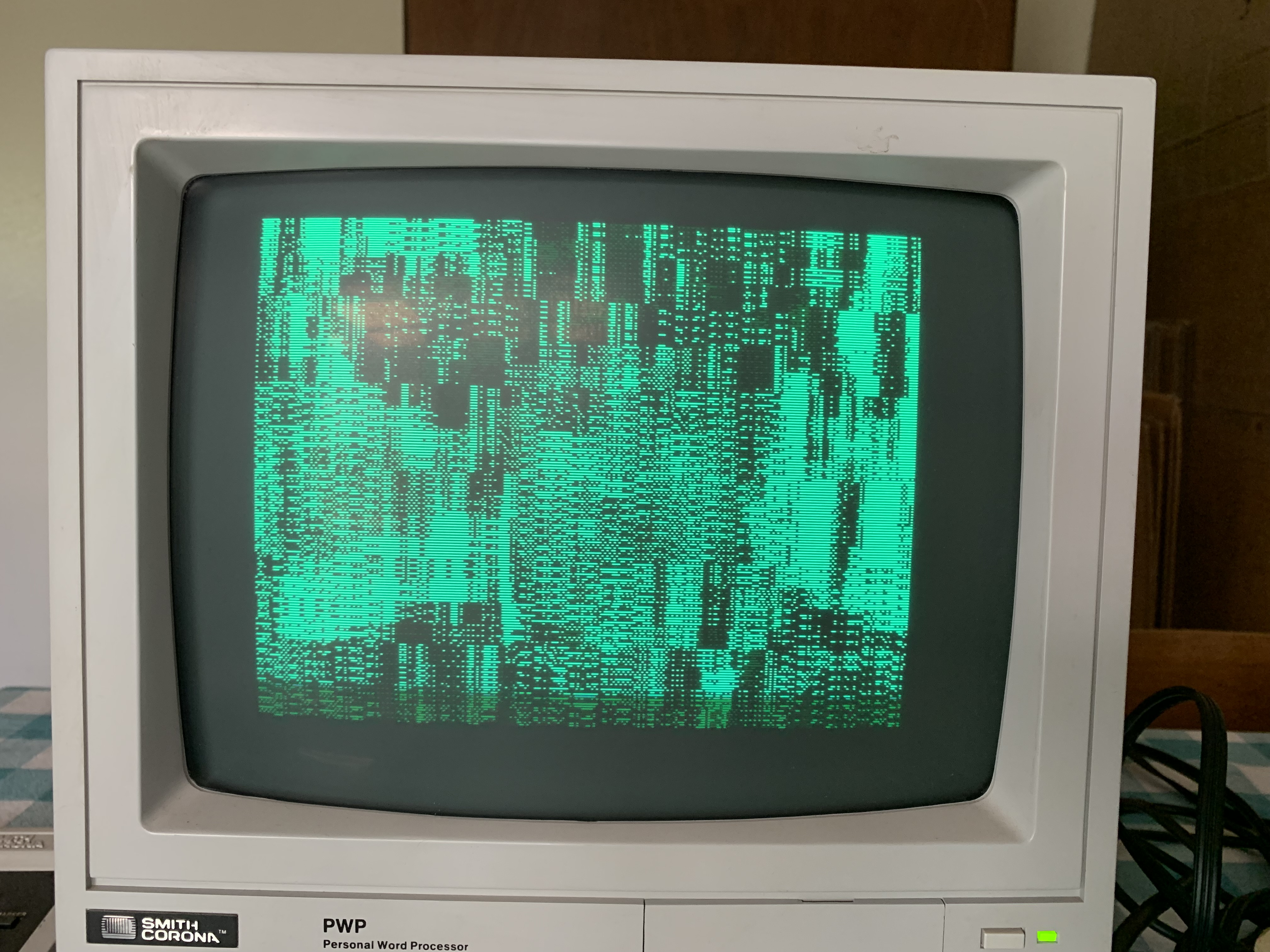 Corrupted picture of TEX
The program loaded and ran, slowly loaded each image on the screen, then copied each image off to the RAM on the S’Card. After loading all eight demo images it then switched to slide show mode and would copy an image back from the S’Card into the Apple II hi-res space as quickly as it could. It didn’t crash while doing that, and while the images were very clearly corrupted, they were also still recognizable. That told me that the card wasn’t completely broken, and there was still hope to repair it.
The way the card manages 1MB of RAM is different than the Apple Memory Expansion and Applied Engineering RAMFactor cards. Those cards use a “slinky” method of accessing the RAM serially through a single IO address one byte at a time. The S'Card emulates a Language Card with multiple banks. A Language Card has 16k, but has to fit in 12k of space. Language Crad RAM is not accessible from BASIC, and it is tricky to access from the Monitor ROM since when Language Card RAM is switched in for reading it occupies the same address space as the Monitor ROM.
Hoping to get some hints about where the problem might be, I started looking at other programs that would check a Language Card for problems. I thought that if I could get the first 16k working then I would be much closer to getting the entire card working. I ran the Apple II Plus Dealer Diagnostics, and it told me that all the RAM was bad. It also provided some information on what it thought was going on with the bank switching. Booting a DOS 3.3 System Master would see the presence of a Language Card and it would try to load Integer BASIC into it, but once it was done typing `INT` would say `LANGUAGE NOT AVAILABLE`.
I found another program which had been written at some hackathon which didn’t believe a Language Card was installed but would let me force running a test on it anyway. It also reported all kinds of bad RAM.
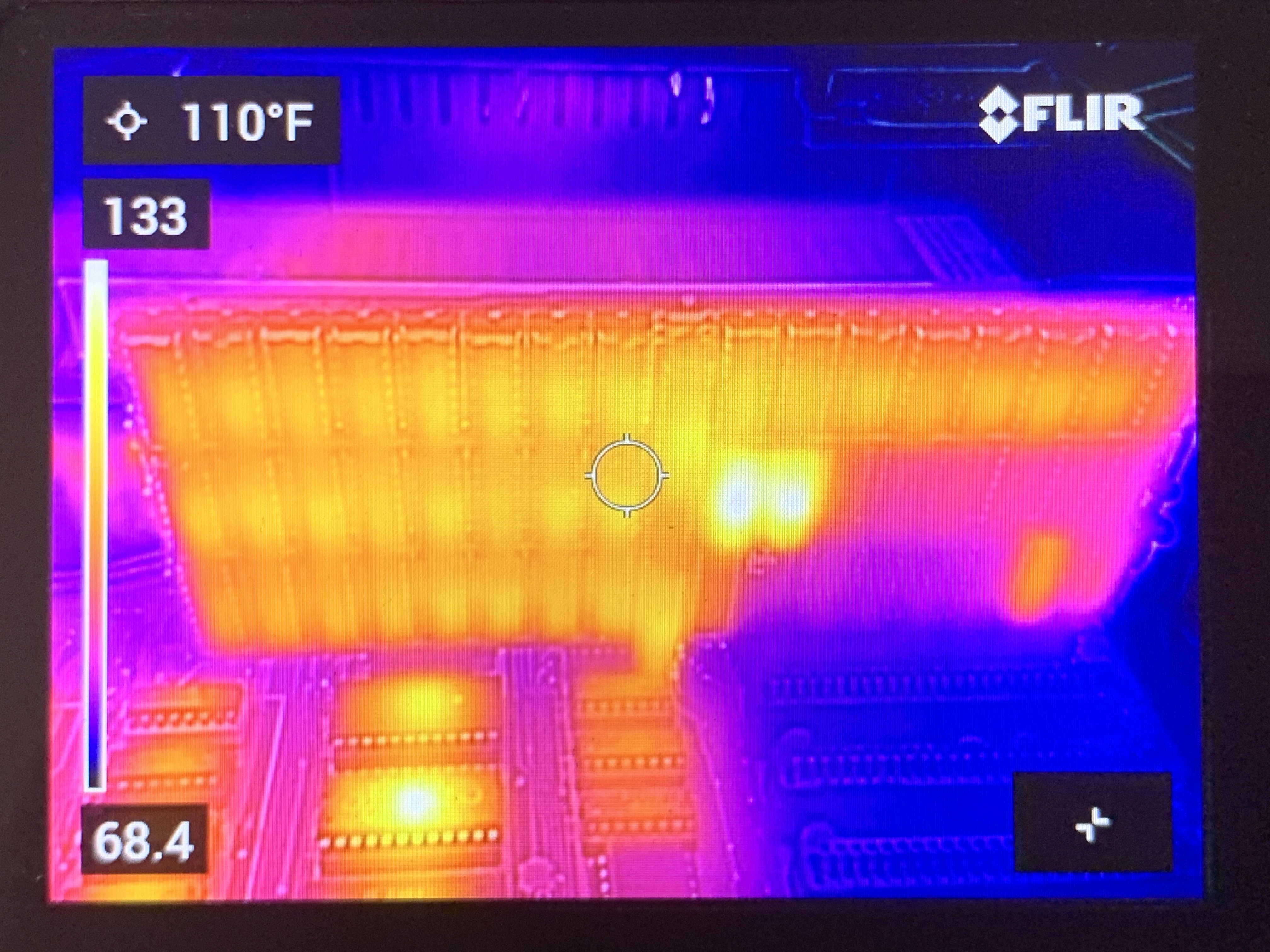 Thermal image of board running in Apple II Plus
Stumped, I decided to try out the thermal camera. Looking at the card I could see two chips that were running much hotter than the others, but not so hot that you couldn’t easily hold your finger on them. Both chips were 74S257 multiplexers, and I happened to have a tube full of them. I swapped them out, put the card back in the II+, booted up the hackathon RAM tester, and it came back and reported the card was good! I had fixed it! Wait, not so fast.
The next thing to try was to see if more than the first 16k of RAM was working so I went back to the slide show demo. It loaded the eight images and started shuffling through them, and while there was a lot less corruption, there were still problems. Some images looked fine but others seemed to have groups of rows swapped all around. Looking closer I could see that every group of 4 lines seemed to be swapped. Odd.
 Uncorrupted watch picture
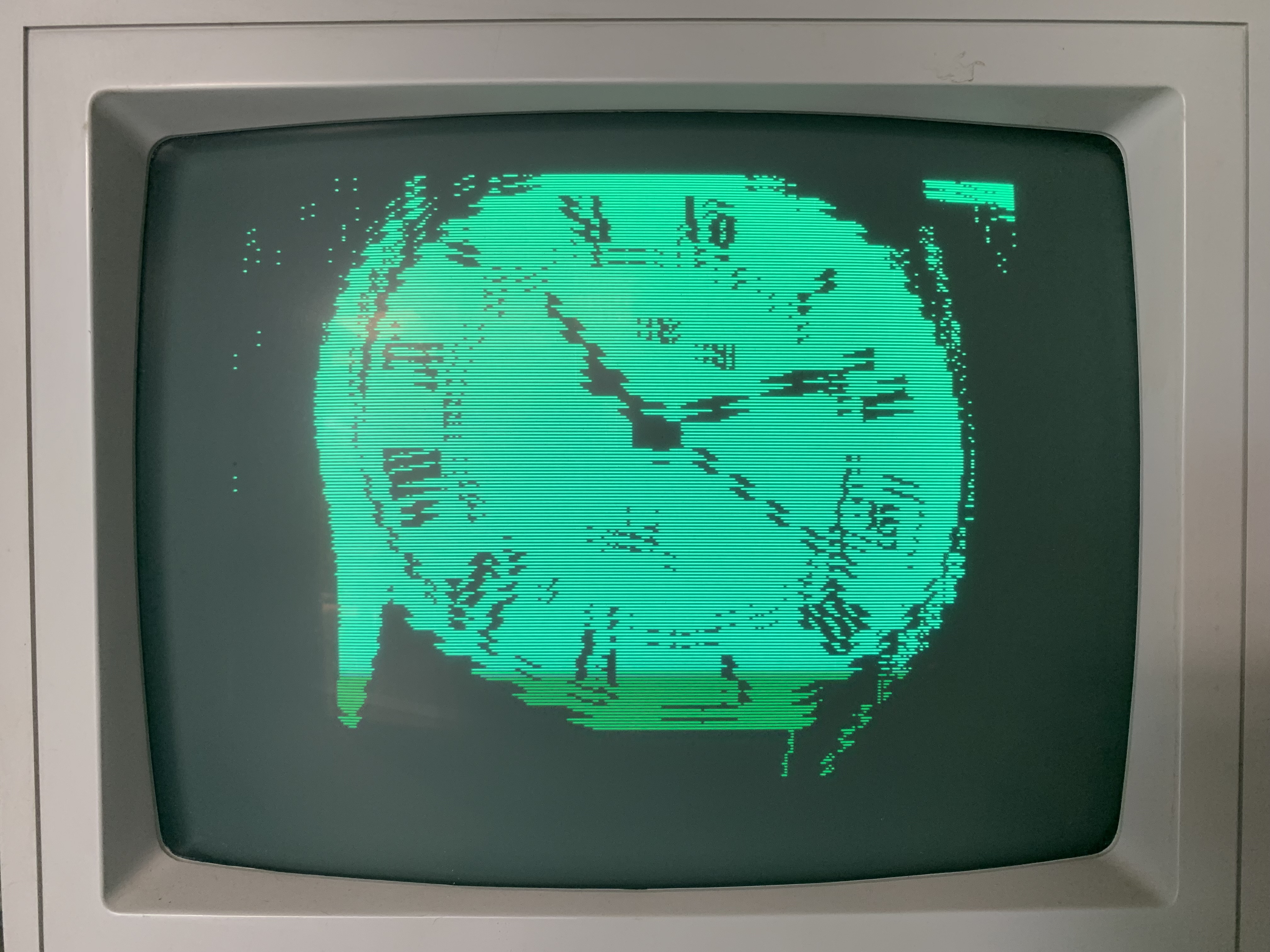 Corrupted watch picture
HGR arranges the screen RAM in an interlaced setup. Anyone that has loaded an image from disk direct to RAM while the hi-res mode is at least somewhat familiar with how the lines don’t load one after the other but instead all over the place. There is a pattern to it though, and RAM is arranged so that 4 lines are all together, with the lower 4k and upper 4k representing every other group of 4 lines. For the lines to be swapped it seemed that two of the 4k banks in the 16k of Language Card RAM were somehow getting swapped.
 Uncorrupted diagnostic image
 Corrupted diagnostic image showing ever 4 rows is doubled
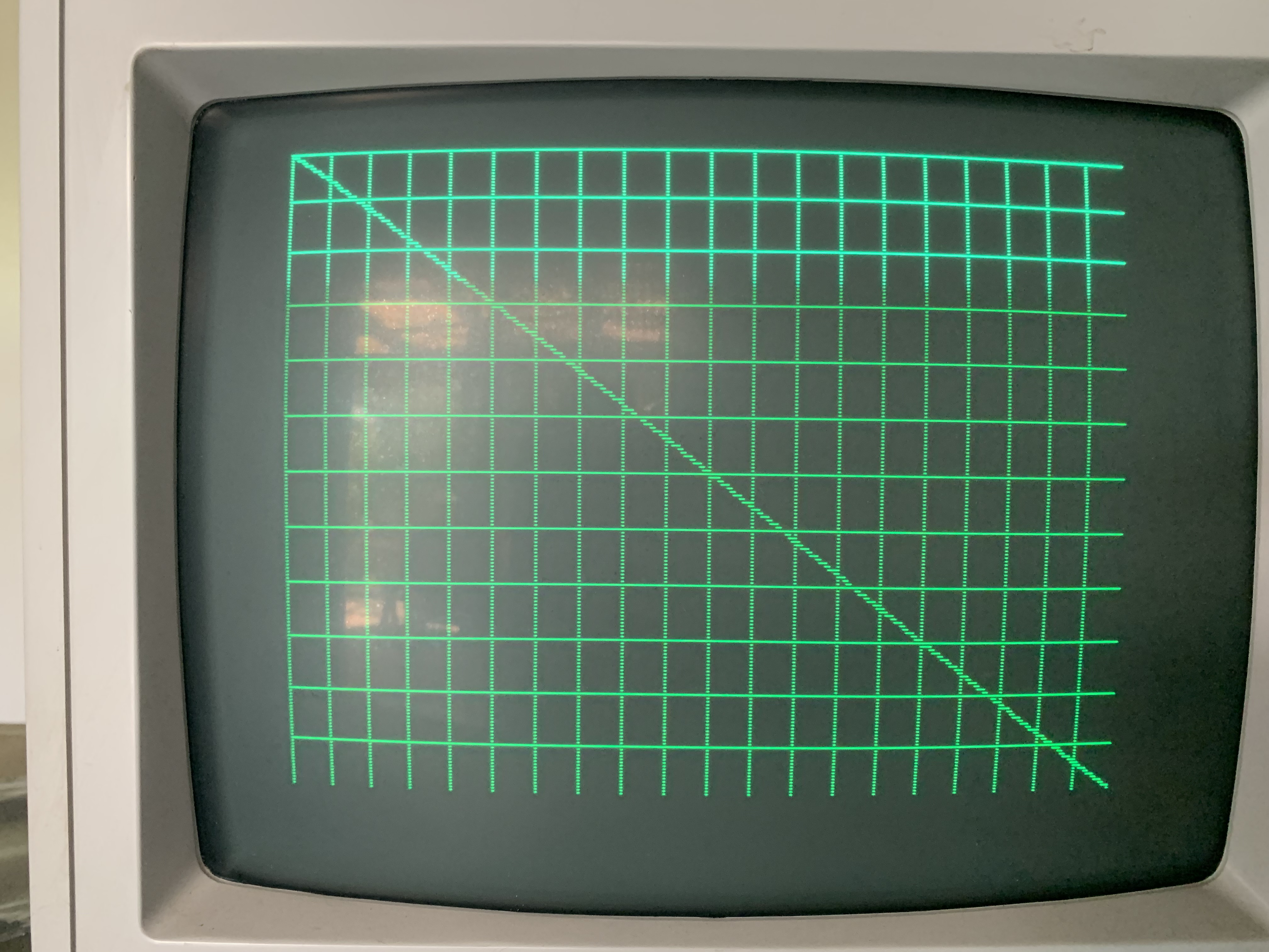
I slapped together a simple image with a grid and a single diagonal line through it to try to get a better idea of which way the swapping was happening. I loaded my “diagnostic” image into several slots on the slide show viewer, and as I cycled through each image, I could see that the first image would be corrupted, the second image would be fine, the third image was corrupted again, fourth was fine, etc. That made sense to me since 8k can be accessed as a single chunk from $E000-$FFFF, and the other 8k has to be swapped between two 4k banks at $D000-$DFFF. What I also discovered was that the rows in a corrupted image weren’t getting swapped, they were being duplicated. So one of the 4k banks wasn’t getting selected at all.
At this point the only way I was going to be able to proceed was to start reverse engineering the circuit. Since I was looking for the logic that handled the soft switches for selecting banks, I started out by tracing where the address lines went. I quickly discovered it wasn’t going to be that simple and relegated myself to tracing out how all the ICs were connected. Luckily there aren’t very many passive components so I was able to use the multimeter in continuity mode to beep out most of everything. Slowly the schematic in KiCad began to grow. Because of the tedious nature of it, I could only do it for so long before needing a break, and getting the bulk of it done took a little more than a week.
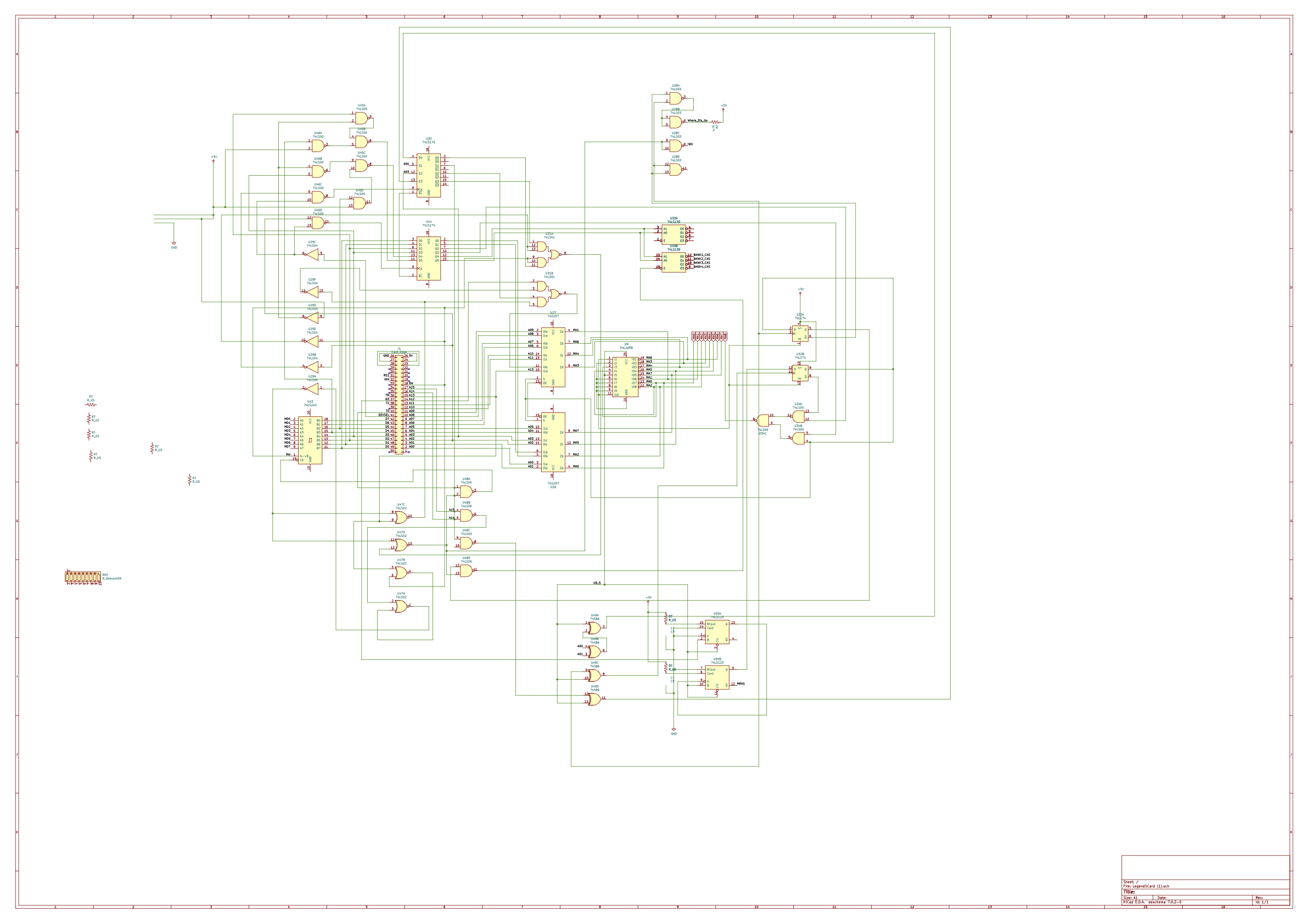 Spaghetti schematic
Of course the schematic I had created in KiCad was a huge tangle of spaghetti. At first I had tried to keep things organized but with so many symbols being added it didn’t take long for things to become a mess. I dropped symbols down anywhere I had room and then would route the wires to link them. The only thing I would do was try to make sure that a wire I was connecting didn’t accidentally get linked to the wrong thing. With things such a mess though it was going to be impossible to try to work out the logic. Re-arranging symbols after wiring them up is quite difficult in KiCad. If you move a symbol it can either be moved by itself and leave the wiring behind losing track of the connections, or it can stretch the wires. But if the wires happen to overlap something when dropped, they will link themselves to that. Either method of moving things ran a huge risk of losing all the connections I had so tediously traced out. But I had to clean it up somehow.
My solution was to go around and put signal names on every single output pin. For ones that I knew what the signal was (such as ones coming from the Apple II bus) I put those names on all the pins connected to the signal. For the others, I invented signal names based on the chip number on the PCB and the pin number that generated the signal. Then I went around and made sure any inputs also had a label matching that output signal name. Once every single pin had been labeled with a signal name, I started deleting the wires. But I didn’t just delete them, I would hook the meter up to both the input and output pins in the connection, verify that they really were connected, and then delete the wire.
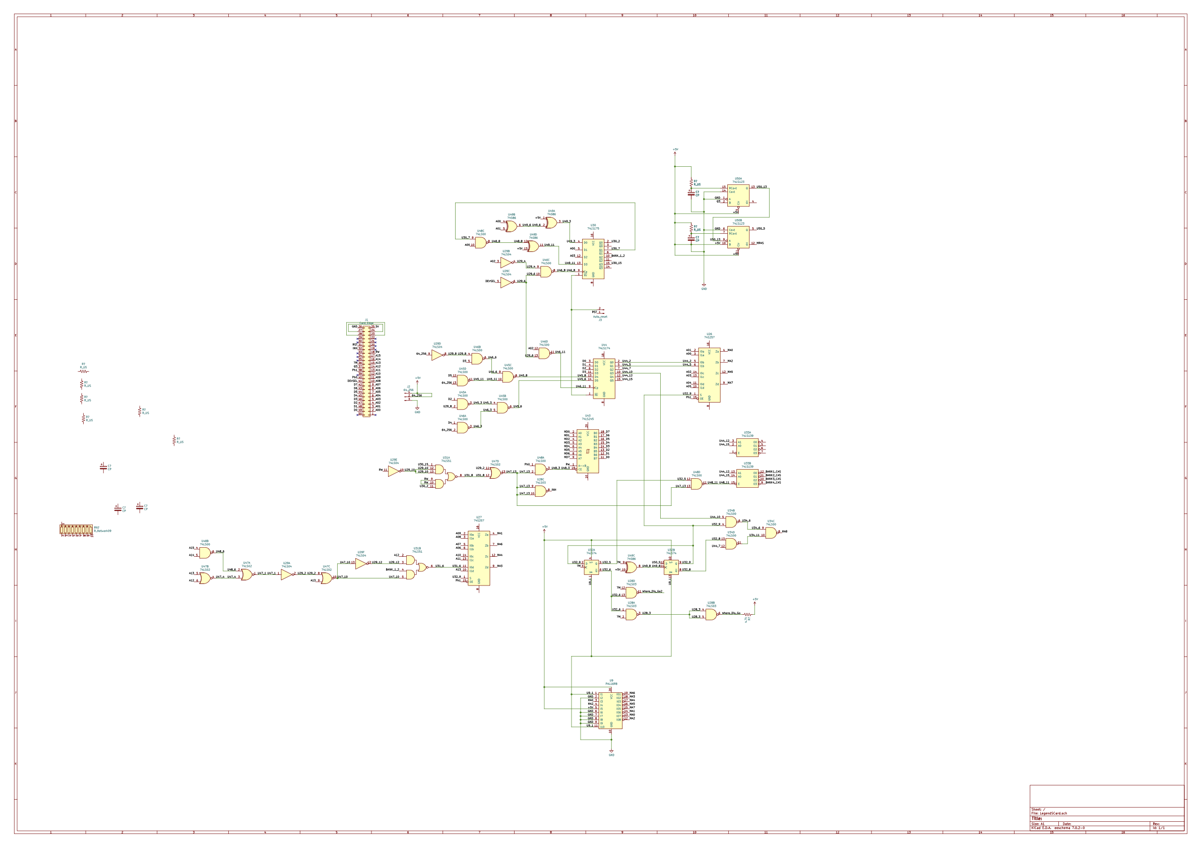 Cleaned up schematic
With every single pin labeled and all the wires gone, it was much easier to start moving symbols around into groups of things that were connected and still larger groups of what seemed like a particular function. After putting symbols near to their connections, I also put back some of the wires, keeping the signal labels on everything. Again very tedious work and t took a couple of days to get the schematic cleaned up.
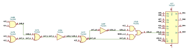 Bank select logic
Since I had a general idea of where I thought the problem was I started going through the schematic trying to understand the logic and which chips controlled which function. Selection of which 4k bank to put at $D000 was determined by whether the low order nibble of the soft switches at $C080-$C08F. Hitting any address from $C080-$C087 selects one 4k bank, $C088-$C0FF selects the other. That meant that A03 was the key, and I traced that through the schematic and found four chips involved in the logic: a 74LS00 NAND, a 74LS02 NOR, a 74LS04 NOT, and a 74LS51 AND/OR inverter.
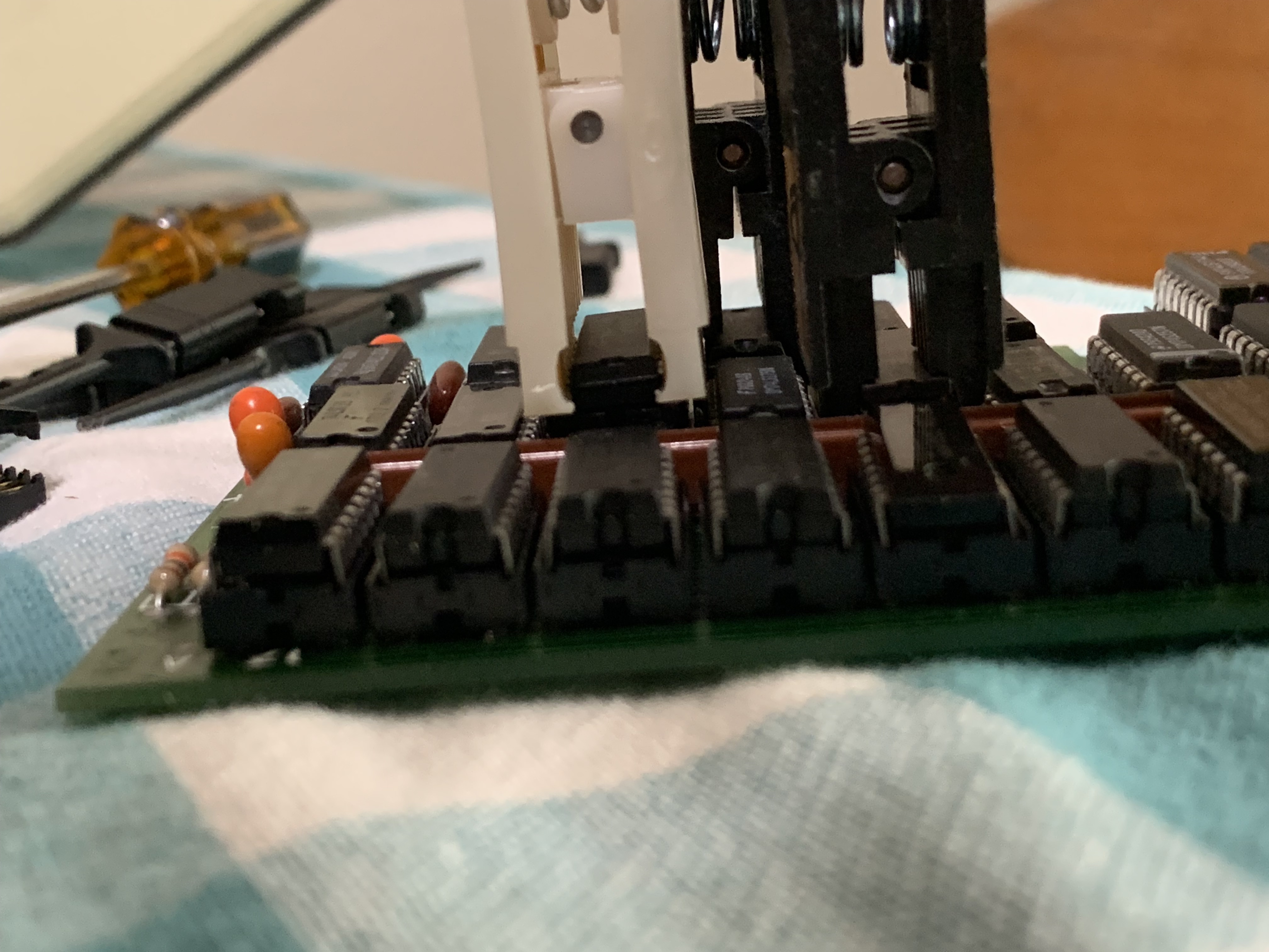 Booster seat for chip to allow clip to fit
Testing the chips while running in the computer seemed like the only way I was going to narrow down the problem which is exactly what a logic analyzer is for. But there were a lot of signals I wanted to monitor, and those little clips that go onto individual pins were getting packed close to one another and kept popping off. I went digging through my chip clips to see if I had some that were the right size and found I have a couple of 8 pins, a 16 pin, and an 18 pin. Close enough. But the chips on the PCB are packed so tightly together that I couldn’t get the clips in where I needed them! I found that the 18 pin one had a narrower edge on the clip and I could squeeze it in between the chips. But the 16 pin that I needed to get the rest of the signals just wouldn’t fit. Solution: booster seat! I popped out the 74LS51 at U31 and plugged it into a 14 pin socket and then put the whole stack back on the card. That raised the chip up enough to get the clip on.
 U31_6 looks fine with BANK_1_2 low
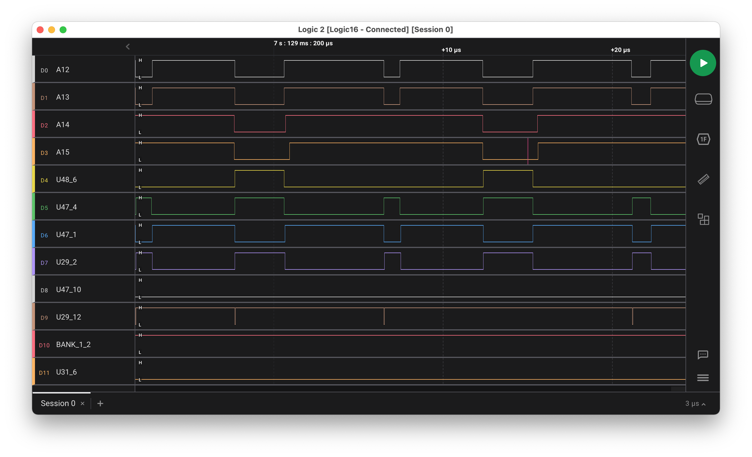 U31_6 stuck low with BANK_1_2 highCs on breadboard
The output at U31 pin 6 looked perfect when accessing $C081, but when accessing $C089 the signal would get locked low, no matter whether or not $D000 was being accessed or not. Definitely not right.
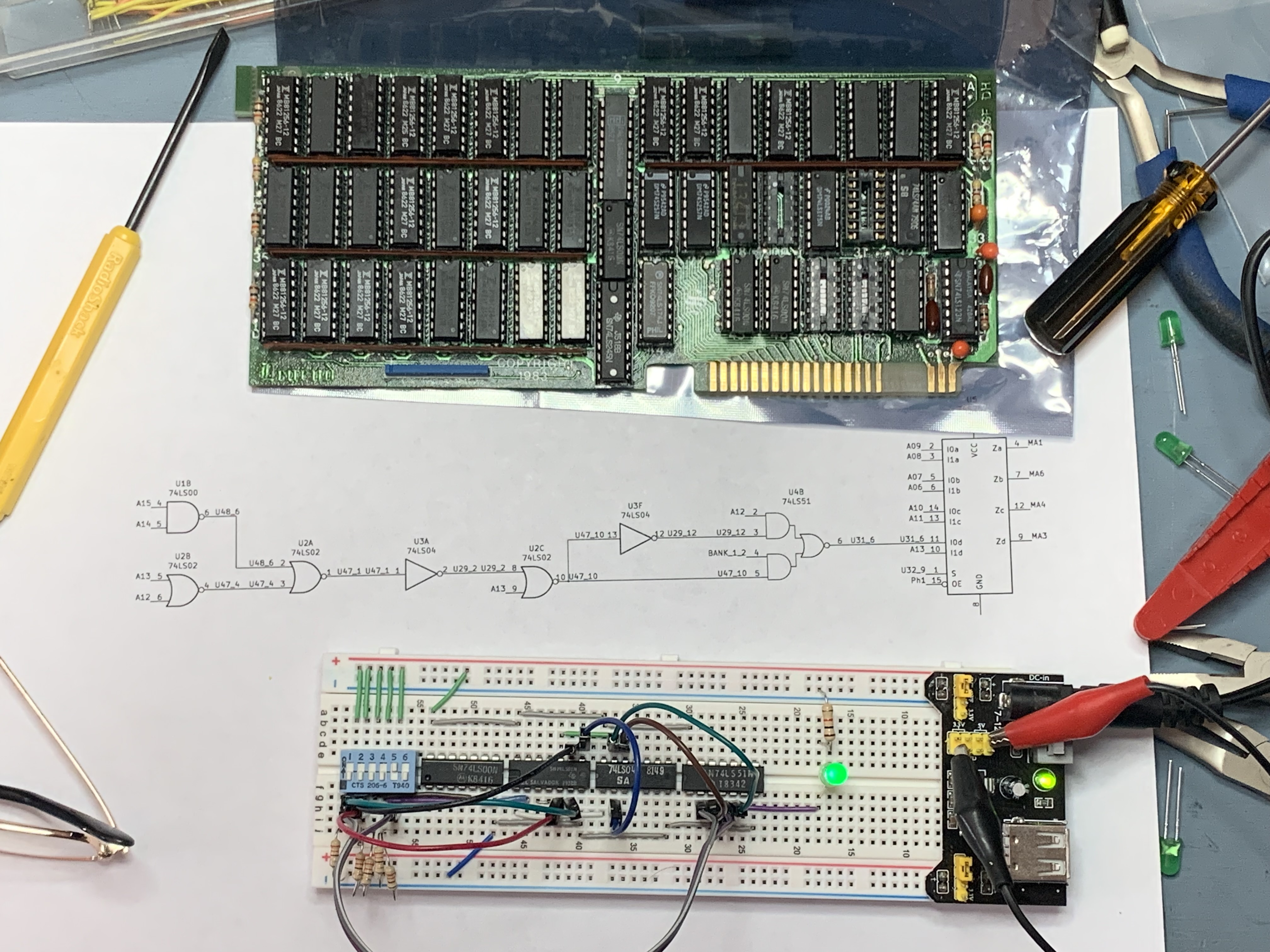 Testing ICs on breadboard
Unsure if I was misunderstanding the logic or if there was a problem, I built a replica of the logic on a breadboard with some switches to act as A12-A15 and the BANK_1_2 signal. I put an LED on the output of pin 6 of the LS51 so I could easily see what happened as I changed address and bank selection. It worked exactly as I expected, with the BANK_1_2 signal only controlling the LED when an address in the $D000 range was simulated. I pulled the chips from the card and swapped them onto the breadboard and they worked correctly too. What gives?
I started to wonder if the 74LS51 was somehow being influenced by a signal from one of its other pins so I lifted pin 6 from the socket and tied it to ground. Examining the state of everything with the logic analyzer showed that BANK_1_2 coming into the 74LS51 was now always low, no matter the state of the soft switches. Yet when I accessed $C089, the output was still getting locked low. Definitely getting influenced by something, but what?
The next thing I tried was lifting the output from the flip-flop while leaving the input on the 74LS51 isolated and tied to ground. No change! Accessing $C089 was still locking the output from the 74LS51 low! Impossible!
Searching all over my schematic showed there was nothing else connected to the BANK_1_2 signal. It went straight from the output of the flip-flop over to the input on the 74LS51. Nothing else did anything with A03, so what else could there be that would be influencing something? Then I noticed that the 74LS175 flip-flop at U30 has two outputs from A03: Q2 and /Q2. Could /Q2 be connected somehow to the 74LS51? Another probe with the multimeter revealed no connection from /Q2 to any of the inputs on the 74LS51.
Easiest way to really check if /Q2 was doing somethiwas to lift /Q2 from the 74LS175. Suddenly I got the results I was looking for! Accessing $C089 was no longer locking the output low! I quickly put back pin 10 of U30 and pin 6 of U31, installed the card, and ran the Legend diagnostics on the first 16k. No address errors! I then let it run the full 1MB test and everything passed!
 Everything passes!
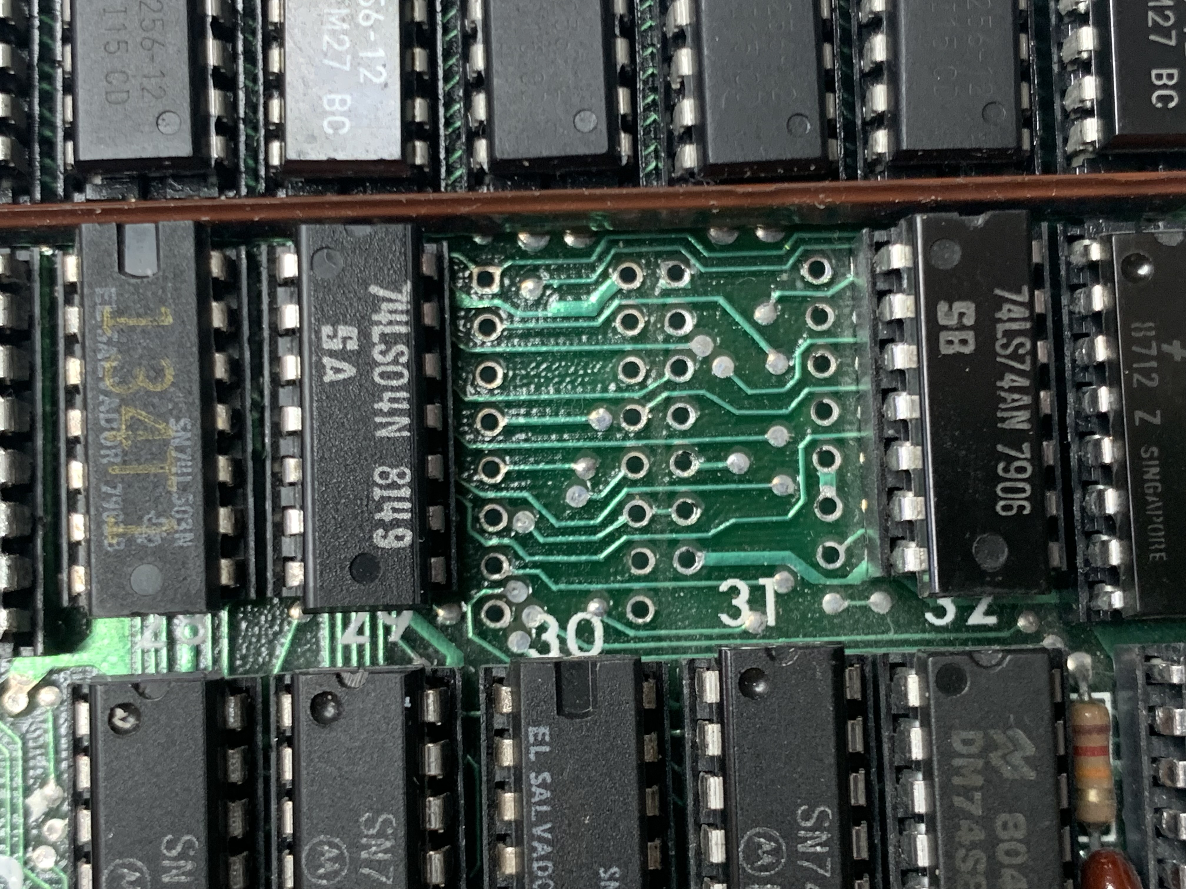
Of course I had to know why that was the fix. I hooked the meter to the pad for pin 11 of U30 and slowly tried each pin to see what it was tied to. It didn’t take long to see that it was connecting to pin 11 on U27, which then connects to pin 6 on U31. Did a piece of metal fall into the socket and it was causing a short? I removed the sockets for U30 and U31 and all was revealed: the board was designed wrong! The trace running from pin 6 of U30 over to pin 11 of U27 was also connected to pin 11 on U30!
 Board made wrong!
The board NEVER worked! It was designed wrong! How did this card get made? Did they never test their design? Did they not even bother to do any testing of the cards before shipping them out? Did they always install the flip-flop at U30 with pin 11 lifted? Do I have a prototype that had never made it to production? From what I can tell, this is the second iteration of the card. My card uses a 20 pin PAL instead of a 24 pin one, the top four holes are unused. The photo of another S’Card I can find shows the larger PAL. The advertisement I found shows the 20 pin PAL16R8.
I could cut the traces going to the wrong pin and solder on some hodge wires, but I think that will be sloppy. Another solution might be to remove the socket for U30 and extract only pin 11 and put it back. But for now I will just leave the traces and sockets intact and keep pin 11 on the IC bent out so it doesn’t make contact.
Now, what’s the best way to make use of 64 Language Cards in an Apple II Plus?
-

-
Legend Industries S'Card
-
Corrupted picture of TEX
-
Memory test fail
-
Thermal image of board running in Apple II Plus
-
Memory test pass
-
Uncorrupted watch picture
-
Corrupted watch picture
-
Uncorrupted diagnostic image
-
Corrupted diagnostic image showing ever 4 rows is doubled
-
Spaghetti schematic
-
Cleaned up schematic
-
Bank select logic
-
Booster seat for chip to allow clip to fit
-
Testing in computer
-
U31_6 looks fine with BANK_1_2 low
-
U31_6 stuck low with BANK_1_2 highCs on breadboard
-
Legend Diagnostic
-
Testing ICs on breadboard
-
Socket leg bent out
-
Testing in computer with pin tied to ground
-
U30 pin 11 shorted to U30 pin 6
-
Pin 11 of U30 bent so it doesn't make contact
-
Everything passes!
-
Board made wrong!


 Recent Toots